

Innovation Photonics Evolution Research Center has installed the following devices with the budget of the project “Development of the Center for International Scientific Innovation by Academia-Industry Cooperation, Fully Utilizing Local Resources, etc.”
These 5 devices can be used according to the Operation Procedure of Devices of “Shizuoka University Innovation Photonics Evolution Research Center”.
Application for using Devices

This system is used for the development of wideband real-time infrared spectroscopic microscope.
In concrete, it is used to evaluate the fitness of quantum cascade laser and investigation of intermolecular interaction of biopolymer.
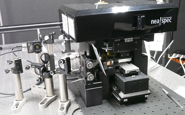
| 〈Manufacture〉 | Neaspec |
|---|---|
| 〈Specification〉 |
|
| 〈Location〉 | Room 429, Innovation Photonics Evolution Research Center Building |

The detector for far-infrared wavelength zone is used in the development of high precision terahertz spectrometry device.
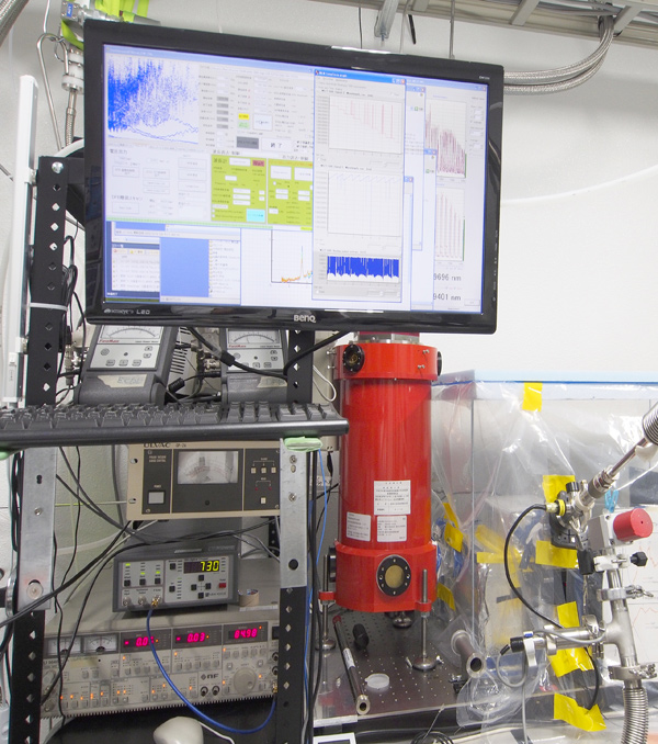
| 〈Manufacture〉 | QMC Instruments Ltd. |
|---|---|
| 〈型 番〉 | QNbB/Dry |
| 〈性 能〉 | System optical responsivity 168kV/W System RMS output noise at 80 Hz 430nV/√Hz System optical NEP at 80 Hz 2.6pW/√Hz |
| 〈Characteristics〉 |
※As a High Precision Tera Hertz Spectrometry Device
|
| 〈Location〉 | Room 210, Innovation Photonics Evolution Research Center Building |

Electron Beam Lithography can formulate patterns of nanometer with high resolution and highly precise positioning. This equipment is mainly used in “Investigation on Functional Light Source Utilizing Microstructure of Semiconductor,” “Study about Optical Function Element Utilizing Metallic Microstructure,” and “Electronic Function Elements Utilizing Microstructure of Semiconductor.”
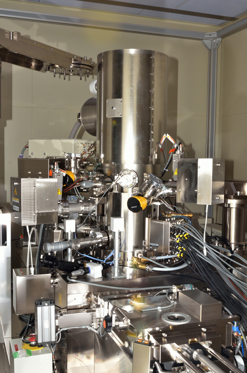
| 〈Manufacture〉 | JEOL Ltd. |
|---|---|
| 〈型 番〉 | JBX-6300SP |
| 〈Specification〉 | Acceleration Voltage 100kV/50kV/25kV Electron Gun ZrO/W Maximum Clock Frequency of the Electronic Line Scanning 50MHz Substrate Size 200mm in Maximum |
| 〈Characteristics〉 |
|
| 〈Location〉 | Room 101, Innovation Photonics Evolution Research Center Building |

This system probes image sensor elements in the state of wafer, and test the functionality in shading/light irradiation state.
Mainly it is used in “Development of High Resolution Infrared Spectrometric Imaging System,” “Development of Super-High Sensitivity/High Function Bio-Imaging Technology,” and “Remote Reproducing Technology based on Super-High Definition Image/3D Image Sensing/Sound Image Control.”
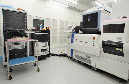
| 〈Manufacture〉 | Prober, Tokyo Seimitsu Co., Ltd. Tester, Teradyne Inc. Light Source, Oyo Electric Co., Ltd. |
||||||
|---|---|---|---|---|---|---|---|
| 〈型 番〉 | Prober, UF3000EX Tester, IP750EX Light Source, AW1053L |
||||||
| 〈Characteristics〉 |
|
||||||
| 〈Location〉 | Room 224, Innovation Photonics Evolution Research Center Building (in the clean room on the 2nd floor) |

The laser direct drawing device is used in prototyping of neutron, X-ray, terahertz detection elements, imaging devices, parasitic sensors, etc.
It mainly addresses subjects of “Paradigm shifts in industrial and medical fields with light sources with the wave surface controlled,” “Innovation of infrared spectrophotometric technology and investigation into intermolecular interactions,” “Implementation of revolutionary technology of formulating time-space image (imaging),” and “Innovation of optical time-space remote control (optic remote) technology.”
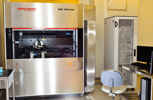
| 〈Manufacture〉 | Hidelberg Instruments (Germany) |
|---|---|
| 〈型 番〉 | DWL2000-OAF |
| 〈Specification〉 | Maximum Drawing Area 200×200㎟ Address/Grid 20nm Minimum Drawing Size 0.7μm Drawing Speed 110㎟/m Edge Roughness (3σ) 70nm Homogeneity of CD (3σ) 80nm Alignment Precision (3σ) 80nm |
| 〈Characteristics〉 |
|
| 〈Location〉 | Room 124, Innovation Photonics Evolution Research Center Building |
innovative Photonics Evolution Research Center (iPERC)
3-5-1 Johoku, Chuo-ku, Hamamatsu, Shizuoka 432-8011 Japan
phone: +81-53-478-3271 / fax: +81-53-478-3256